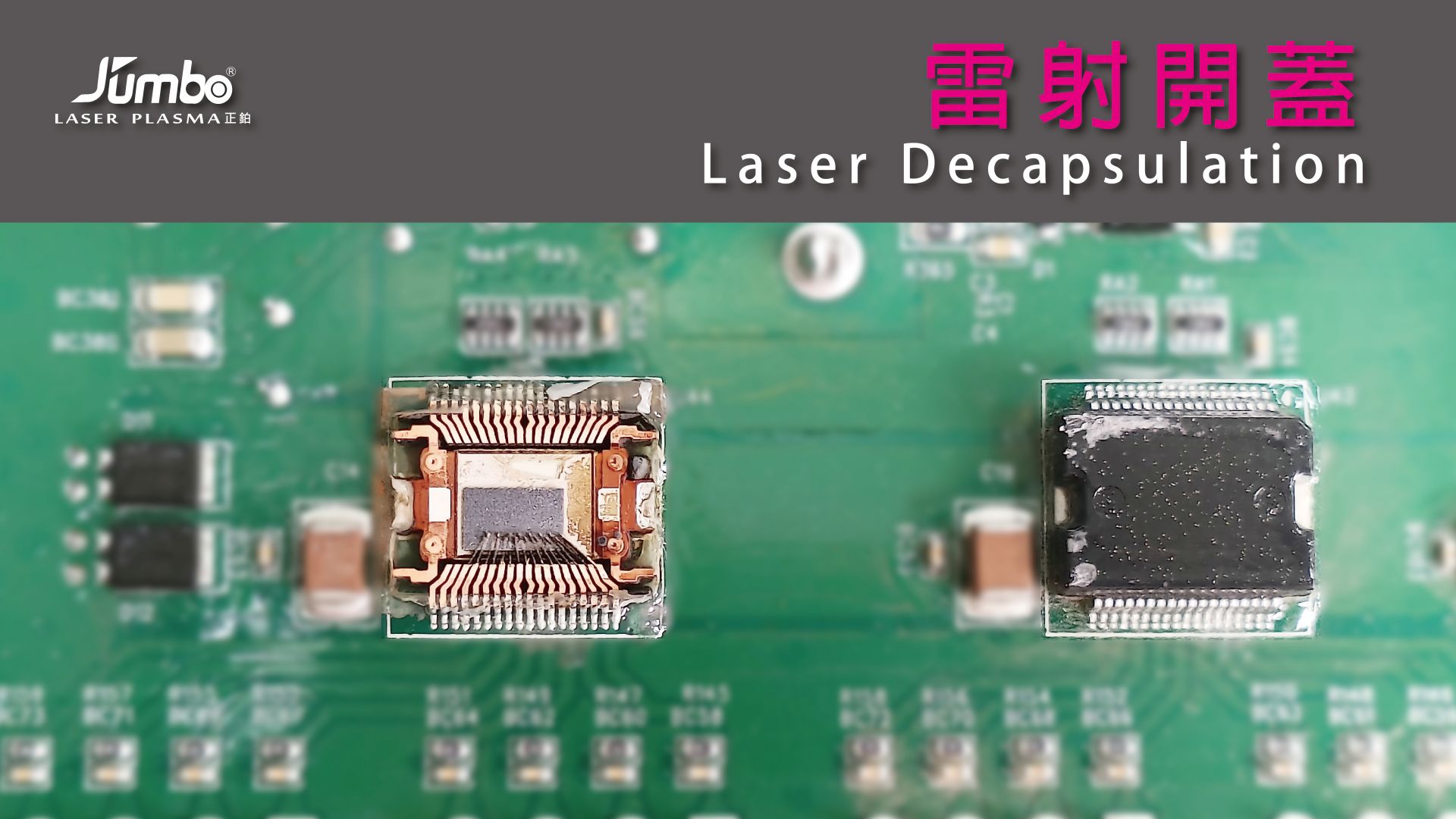
 PCB Laser Depaneling Technology
7 Key Advantages of Using Laser Technology for PCB Depaneling
PCB opening using laser technology has 7 significant benefits
1. High Precision and Accuracy: Laser technology enables extremely high precision and accuracy, achieving superior manufacturing standards for PCB depaneling. This is particularly important for densely packed components or intricate microstructures on the PCB.
2. Non-Contact Processing: Laser depaneling is a non-contact process that does not physically touch the PCB surface, thus preventing surface damage. This is crucial for maintaining PCB surface integrity, especially for high-performance or fine-feature PCBs.
3. High Efficiency and Production Speed: The laser depaneling process is highly efficient and supports rapid PCB production. Its speed and automation capabilities help enhance productivity and reduce lead times.
4. Design Flexibility: Laser technology supports a variety of cut shapes and sizes without the need to change tools or blades. This gives PCB designers more freedom and allows for more complex structures.
5. Reduced Waste: Compared to traditional mechanical processing, laser depaneling minimizes material waste. This contributes to resource efficiency and environmental sustainability.
6. Multi-Material Compatibility: Laser depaneling works with a wide range of PCB materials, including FR4 (glass fiber-reinforced epoxy), metal-core boards, and ceramic substrates, making it suitable for diverse applications.
7. High-Quality Results: Laser depaneling achieves smooth, consistent cutting edges with no burrs, ensuring high-quality PCB production.
Laser processing technology offers an efficient, precise, and contact-free solution for PCB depaneling, while providing excellent design flexibility. These advantages make it a vital tool in modern PCB manufacturing, supporting the production of complex electronic designs with high quality and performance. 
 PCB Laser Depaneling Technology